

The Material Science Behind GaN and GaAs SSPAs: A Technical Deep Dive
Author:Xiamen Lineyi Electronics Co.,Ltd.
Click:
Time:2025-11-08 22:29:29
When selecting a Solid State Power Amplifier (SSPA) for your RF system, the choice between Gallium Nitride (GaN) and Gallium Arsenide (GaAs) semiconductor technologies represents one of the most critical decisions. Each material offers distinct advantages that make it suitable for specific applications. Understanding the fundamental material properties is essential for making an informed choice that balances performance, cost, and reliability.
This technical deep dive explores the material science behind both technologies and how their inherent characteristics translate into real-world performance differences.
Fundamental Material Properties: The Building Blocks of Performance
The performance characteristics of any semiconductor technology stem from its basic physical properties. Here's how GaN and GaAs compare at the material level:
Bandgap Energy:
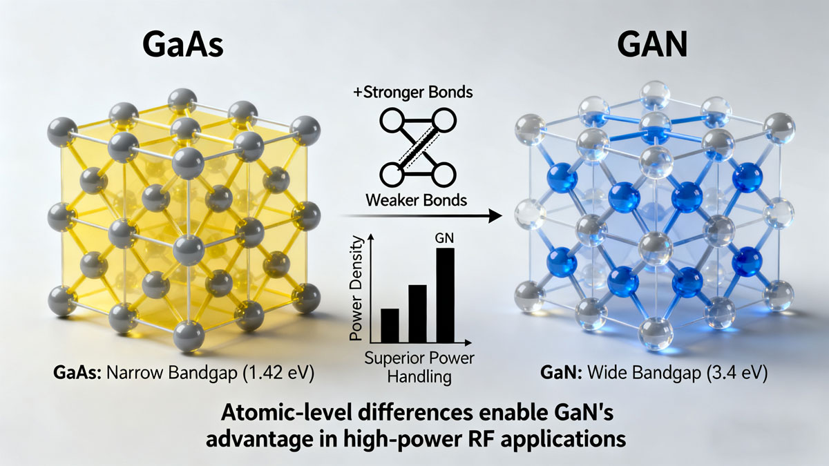
- GaN (Gallium Nitride): 3.4 eV - This wide bandgap is the primary reason for GaN's exceptional performance. It allows GaN devices to operate at much higher temperatures, handle higher power densities, and withstand greater voltage stresses than narrower bandgap materials.
- GaAs (Gallium Arsenide): 1.42 eV - While superior to silicon, GaAs's narrower bandgap limits its maximum operating temperature and breakdown voltage compared to GaN.
Electron Mobility:
- GaN: ~2000 cm²/V·s - High electron mobility enables excellent high-frequency performance and switching speeds.
- GaAs: ~8500 cm²/V·s - Superior electron mobility gives GaAs an advantage in very high-frequency, low-noise applications.
Thermal Conductivity:
- GaN: 1.3-2.0 W/cm·K - Good thermal conductivity allows efficient heat dissipation, crucial for maintaining performance in high-power applications.
- GaAs: 0.5 W/cm·K - Lower thermal conductivity requires more sophisticated thermal management solutions for high-power designs.
Critical Electric Field:
- GaN: 3.3 MV/cm - The high critical electric field enables GaN devices to operate at much higher voltages, directly contributing to higher power density.
- GaAs: 0.4 MV/cm - Significantly lower than GaN, limiting the maximum operating voltage and power density.
Performance Characteristics: Translating Theory into Practice
These fundamental material differences manifest in several key performance parameters:
Power Density and Efficiency:
GaN power amplifiers typically achieve 5-8 W/mm of gate periphery, compared to 1-1.5 W/mm for GaAs devices. This 5x improvement in power density means a GaN-based microwave power module can be significantly smaller for the same output power, or deliver much higher power in the same footprint. Additionally, GaN amplifiers typically achieve 5-15% higher power-added efficiency (PAE) than comparable GaAs designs.
Frequency Range and Bandwidth:
While both technologies support microwave and millimeter-wave frequencies, GaAs maintains an advantage in certain very high-frequency applications above 40 GHz due to its superior electron mobility. However, GaN technology continues to advance rapidly, with current devices operating effectively up to 100 GHz.
Linearity and Intermodulation Performance:
GaAs amplifiers traditionally offered superior linearity, making them preferred for applications requiring complex modulation schemes. However, modern GaN devices have closed this gap significantly through advanced circuit design techniques and process improvements.

Reliability and Ruggedness: Operating in Demanding Environments
The wider bandgap and stronger chemical bonds in GaN give it inherent advantages in reliability and ruggedness:
- Operating Temperature: GaN devices can operate at channel temperatures exceeding 200°C, compared to approximately 150°C for GaAs
- Radiation Hardness: GaN's crystal structure provides inherent resistance to radiation effects, making it suitable for space applications
- ESD Tolerance: GaN devices typically withstand electrostatic discharge (ESD) events better than GaAs components
Thermal Management Considerations:
The higher power density of GaN SSPA technology creates significant thermal management challenges. While GaN itself has good thermal conductivity, most devices are grown on silicon carbide (SiC) or silicon substrates to further enhance heat dissipation. Proper thermal design is essential to realize GaN's full performance potential.
Understanding these fundamental differences provides the foundation for making informed technology selections. In our next article, we'll explore how these technical characteristics translate into specific application advantages across different industries and use cases.
Choosing between GaN and GaAs SSPA technology requires careful consideration of your specific performance requirements and operating environment. Xiamen Lineyi's engineering team has extensive experience with both technologies and can help you select the optimal solution. [Contact us] for a personalized technical consultation.

点击右上角
分享给朋友吧







 Long by picture save/share
0
Copyright © Xiamen Lineyi Electronics Co., Ltd All rights reserved.
点击右上角
分享给朋友吧
